
Image revolutionaries
In selecting the winners of the 2017 Queen Elizabeth Prize for Engineering (QEPrize), the judges have managed to encompass four key stages in the history of solid-state image sensing that are embodied in four exceptional individuals. They are George Smith, who invented the charge-coupled device (CCD); Michael Tompsett, who exploited its potential in image sensing; Nobukazu Teranishi, who came up with the modern pinned photodiode (PPD); and Eric Fossum, who developed the complementary metal-oxide semiconductor (CMOS) sensor. These interlocking developments have had an impact to match the extent of their begetters’ ingenuity. Image sensing has proved to be a technology as socially influential as it is fast moving.
In selecting the winners of the 2017 Queen Elizabeth Prize for Engineering (QEPrize), the judges have managed to encompass four key stages in the history of solid-state image sensing that are embodied in four exceptional individuals
“Any sufficiently advanced technology is indistinguishable from magic,” wrote science-fiction novelist Sir Arthur C Clarke CBE. He was teasing us, but in this context, his wit has a double relevance. While most users of traditional film cameras had at least a dim idea of how their instruments captured light, this is much less true of the billions who reap the benefits of digital imaging every day; and the images themselves, whether a picture of some far distant galaxy or the interior of the human gut, often have an emotional resonance that surely merits the term ‘magical’?
The camera in a pill
💊 Capsule endoscopy to deliver drugs & vitamins
One of the great virtues of the new sensor technology lies in miniaturisation: in this instance, a camera small enough to swallow. Capsule endoscopy, as it is called, relies on a camera, an LED and a transmitter built into a pill of the size commonly used to deliver drugs or vitamins. As it moves through the stomach and the rest of the gut, its camera records images that can be transmitted to a recording device worn by the patient.
Conventional endoscopy relies on a long, flexible viewing tube inserted through the mouth and as far down the digestive tract as it will reach. Capsule endoscopy avoids the inevitable discomfort of this procedure, and dispenses with the need for trained staff to perform the examination.
A capsule camera may be tethered on a fine control wire and retrieved by pulling it back up after examination has been completed. However, as manufacturing costs fall, it can also be disposable and allowed to pass out of the body.
This is still a novel technology, and the extent of its benefits in searching for cancers or other abnormalities of the digestive tract is still being assessed, but findings so far are encouraging.

© GivenImaging
The first digital photos
The story behind image-sensing technology begins with George Smith. In 1959, after graduating from the University of Chicago with a PhD in physics, he joined a department of Bell Telephone Laboratories headed by Canadian physicist Willard Boyle (deceased). In line with the topic of his PhD thesis, he continued to study semimetals such as arsenic, antimony and bismuth. He subsequently moved to another department at Bell titled Device Concepts. In 1969, it was here that he and Boyle invented the CCD.
Boyle and Smith’s intention was to exploit the capacity of semiconducting materials to transfer charge along their surface from one storage site to the next. They reasoned that patterns of charge, created electronically on the surface of a CCD, could be used to store and transfer information of the kind required by computer memories. In fact, the CCD was soon to find its major use in a quite different sphere, but the importance of Boyle and Smith’s invention was self-evident, and celebrated in 2009 when the pair received the Nobel Prize for Physics.
They reasoned that patterns of charge, created electronically on the surface of a CCD, could be used to store and transfer information of the kind required by computer memories
Exploring the universe
🌌 The image sensors crucial to the success of the Euclid mission
Euclid is a European Space Agency mission due to be launched in 2020. Its ambitious aim is to investigate the dark energy that accounts for three quarters of the energy/matter content of the universe, and may explain why the rate expansion of the universe is accelerating.
Crucial to the success of the mission are Euclid’s reliable, lightweight, high-performance image sensors for observing the visible and near-infrared output of the billions of faint galaxies towards which they will be directed. The focal plane of the visible light instrument will comprise an array of 36 CCDs (as seen in the image) designed for the exceptional circumstances in which they will be operating. They are highly efficient, should be able to tolerate the radiation to which they will be exposed, and by generating 25 times as many pixel images as a top digital camera, should offer a far better quality image. Nothing less would allow astrophysicists to probe the history and nature of the universe.
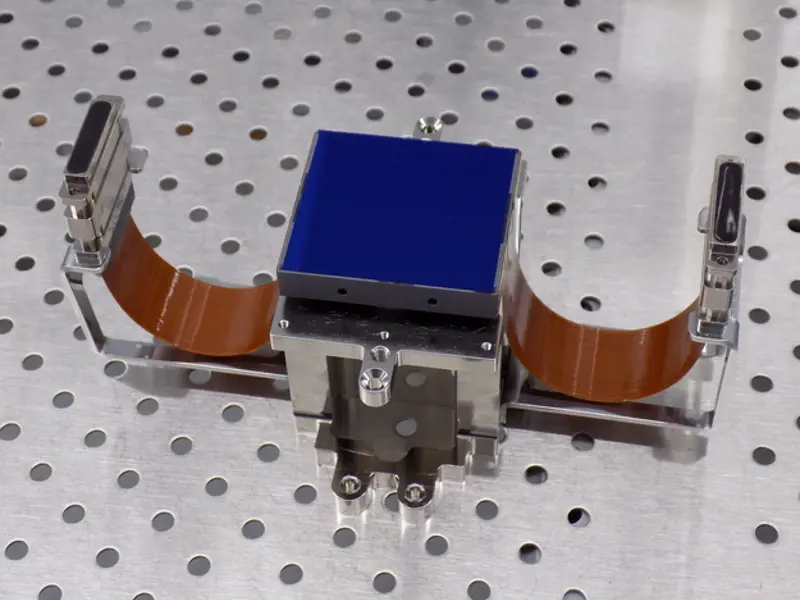
© European Space Agency
The real value of the CCD began to emerge with its change of role from memory storage to image sensing, which is attributable to the second of the 2017 QEPrize winners, Michael Tompsett. Born in the UK, he studied physics at the University of Cambridge and followed it up with a PhD in engineering. By the time he came to work on CCDs, he had already demonstrated his inventiveness. While employed by the then English Electric Valve Company, he devised the uncooled thermal-imaging television camera tube. However, by then the focus of his interests had already begun to change.
“Ideas were being floated about solid-state imagers,” he recalls, “and that was something I wanted to work on.” In 1969, his fascination took him to the best place to be for anyone with such an interest: Bell Telephone Laboratories. He quickly realised how Boyle and Smith’s CCDs could be exploited for their capacity to capture images, and embarked on a quest to develop imaging systems that were much smaller than those in use at the time.
In an image brought to focus on the surface of a CCD, the location and number of electrons form an analogue representation of that image
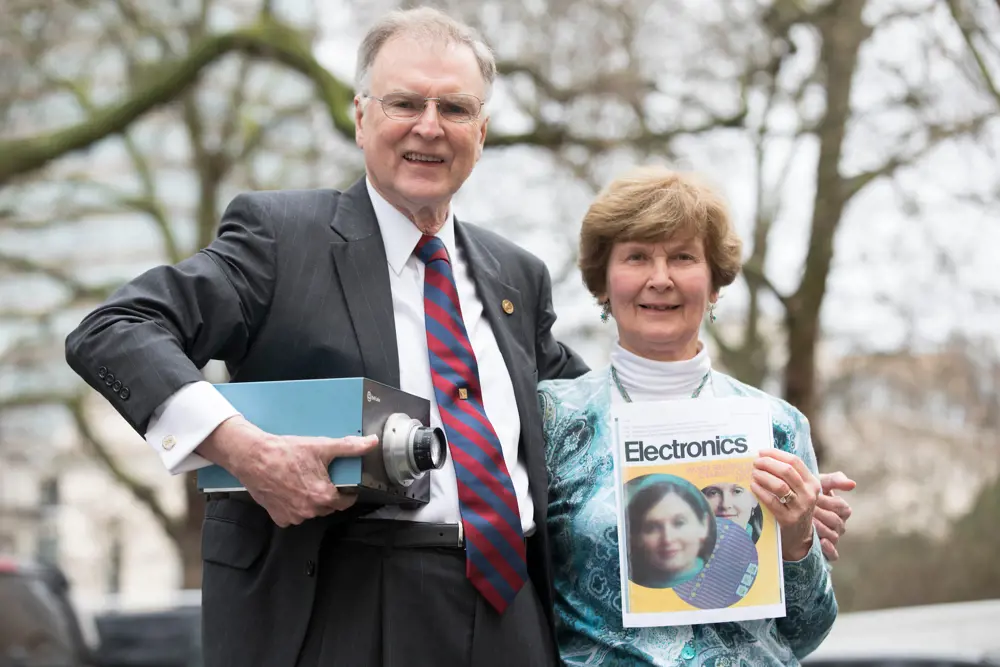
Michael Tompsett holds a colour camera that he helped to develop while his wife Margaret holds a photo of herself, which was the first colour image using three solid-state imagers © Jason Alden
Image capturing by CCDs is a product of their response to light; when photons impinge on the light-sensitive surface of an array of pixels on a silicon chip, they trigger the formation of electrons. These are captured by the electrostatic forces in the pixel and accumulate. The brighter the light, the greater the number of electrons generated within any one pixel site. In an image brought to focus on the surface of a CCD, the location and number of electrons form an analogue representation of that image.
Besides acting as a photodetector, the pixel structure of a CCD also serves as a readout system. Charge generated in the pixels is transported, step-by-step, from one site to the next, across the array to one corner of the chip. Here, Tompsett added to the original CCD design with an analogue-to-digital converter to turn the amount of charge generated within each pixel into a digital value to be memorised. The digital readout so compiled forms a numerical description of the image. “I led the group that developed CCD images, and made the first colour camera,” Tompsett says. “And I took the first colour pictures,” he adds. “The first person to have a digital image taken of her was my wife.”
“I led the group that developed CCD images, and made the first colour camera,” Tompsett says. “And I took the first colour pictures,”
Hands-free imaging technology
🥽 Motion sensing and mixed reality headsets for gamers
In 2010, Microsoft released its motion-sensing device, Kinect. Kinect was an instant hit, selling more than eight million units in its first two months on sale and becoming the then fastest-selling consumer electronics device in history. Combining depth sensing and digital image sensors with machine learning, the gadget dropped gamers right into the action by turning their bodies into controllers.
At the time of its launch, Kinect’s learning technology was so advanced that it earned the engineers behind it the 2011 MacRobert Award, marking it as the ‘next big thing’ in engineering. Although Microsoft announced in 2017 that it was ending production of Kinect, its groundbreaking technology lives on.
HoloLens, Microsoft’s ‘mixed reality’ headset, incorporates depth-sensing technology and the latest in digital imaging sensors to capture the wearer’s real-world environment. The device then places holograms directly onto physical objects within their field of vision to enhance reality.

© Microsoft HoloLens
Improved quality and smaller
Tompsett had followed his father into engineering, and Nobukazu Teranishi also had a father who worked in the field. It was nuclear fusion that first attracted him, but that gave way to more basic physics and, when he joined the NEC Corporation in 1978, to image sensing. Photodiodes of that period were plagued by deficiencies such as noise and image lag, so Teranishi set out to unravel the roots of these problems and looked for a means of dealing with them. Two years after joining NEC, he invented the PPD.
Conventional photodiodes comprise a p–n (positive–negative) junction at the boundary between two types of the same semiconductor crystal. The ‘n’ side contains an excess of electrons, while the ‘p’ side contains an excess of holes. Teranishi added a p layer with a high level of impurities on top of the n layer of a normal photodiode. This modification had the effect of eliminating image lag, reducing dark current (the current generated even in the absence of light) and producing a much better image quality. It allowed pixel sizes to be reduced and their numbers increased, with a consequent boost to resolution. Mass production started in 1987, and a few years later, CMOS image sensors could also benefit from the use of PPDs.
Teranishi added a p layer with a high level of impurities on top of the n layer of a normal photodiode. This modification had the effect of eliminating image lag, reducing dark current (the current generated even in the absence of light) and producing a much better image quality
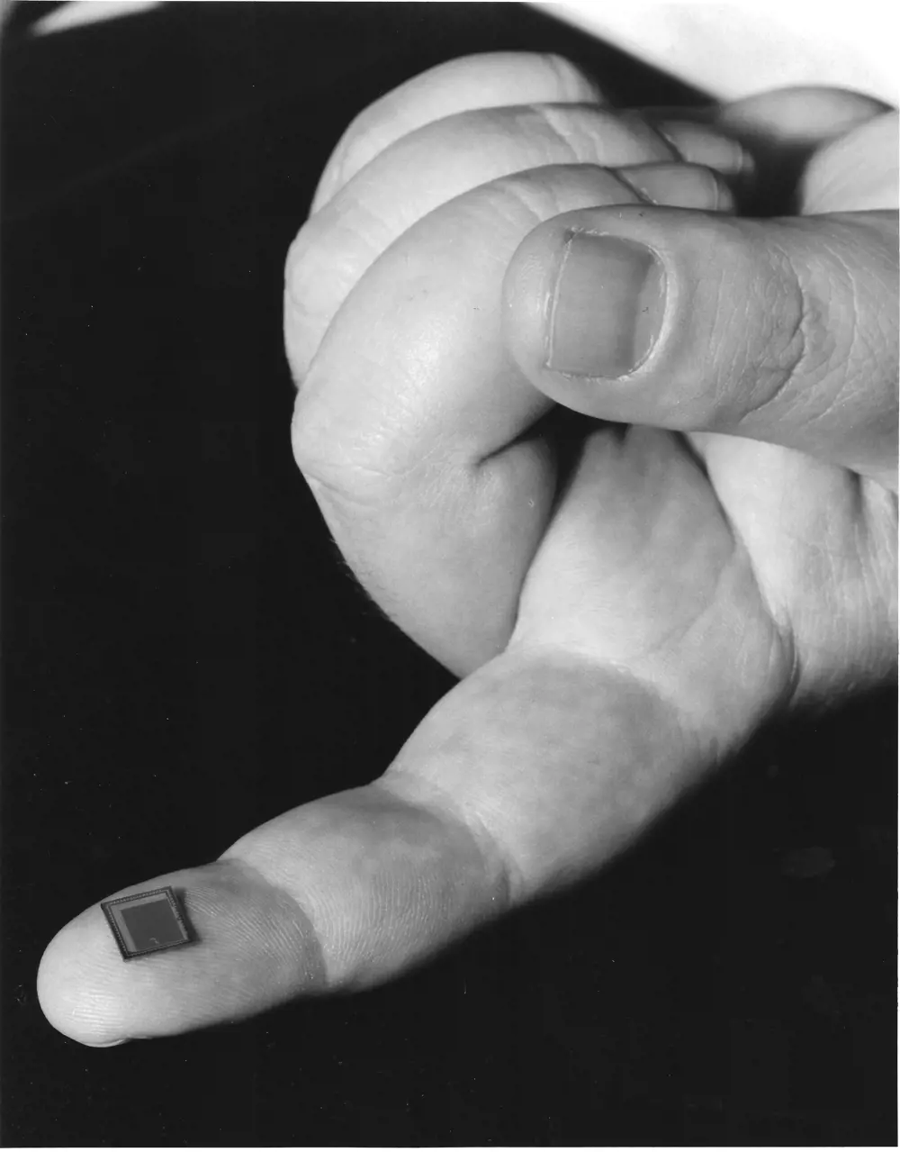
CMOS sensors paved the way for smaller cameras and the development of the ‘camera on a chip’. Although not as high quality as CCD sensors, they use less power and are cheaper to produce. They are also integrated into fingerprint recognition on smartphones and are used for identification in biometric passport booths for border control
Teranishi moved to the Panasonic Corporation in 2000, and subsequently to his present academic posts at the University of Hyogo and at Shizuoka University. Here he works on X-ray image sensors and photon counting sensors.
Eric Fossum too has moved between industry and academia. His introduction to image-sensing technology came while he was still in graduate school, shortly before CCDs began to find a widespread application in consumer products. Having worked on them at Columbia University in New York, he was recruited by NASA in 1990 and moved to its Jet Propulsion Laboratory (JPL) in California. By this time, CCD devices had proved successful in both their consumer and scientific applications, but NASA wanted smaller and less power-hungry CCDs that would also be more robust in a space environment. Fossum’s remedy was to use CMOS microelectronics technology in developing a new generation of sensors.
Instead of transferring electric charges across the array of pixels and reading them at one corner, CMOS sensors use transistors within each pixel to amplify the voltage signal created there. As Fossum is at pains to point out, this is an idea that was first suggested in 1967 (before it could be implemented) by British engineer Peter Noble working at Plessey. CMOS sensors have most of the circuitry and components that they require integrated into the sensor itself (hence the term ‘camera on a chip’) and get by on as little as a hundredth of the power needed by CCDs. While the earliest CMOS devices performed relatively poorly by comparison with CCDs, they have been catching up ever since. CMOS devices are also cheaper to manufacture, and they eventually became the natural choice for small consumer electronic devices such as mobile phones.
Despite their advantages, early interest in the new CMOS sensors was, at best, lukewarm. Fossum left JPL in 1996 having already set up his own company, Photobit, to commercialise CMOS image-sensor technology. He has since returned to academic life and is now a professor at Dartmouth College’s Thayer School of Engineering in New Hampshire. However, he is still engaged in entrepreneurial research; he and a former student have a created a new startup company called Gigajot. “We are working on a possible next generation image-sensing technology where we count each photon of light, one at a time,” he says.
Crowdsourced disease diagnoses
📱 Smartphones as the ultimate crop diagnostic tool
Small, cheap and universally available, digital image sensors have turned smartphones into the ultimate diagnostic tool. PlantVillage is a free, open-access platform that connects crop farmers with a global community of experts, diagnosing plant disease from the other side of the globe.
Farmers use their phones to take a photo as soon as they notice a change in their crops, uploading the image directly to an online database. With a worldwide network of scientists logging in, they can have an answer to their problem within hours. The rapid response allows farmers to quickly control the disease to save not only their own harvest, but others nearby.
The online platform was created by two assistant professors at Penn State University’s College of Agricultural Sciences, and is getting smarter; it learns from an ever-growing image bank and can offer computerised diagnosis.
While still in its infancy, the artificial intelligence matches healthy and diseased leaves, and can so far detect 26 different diseases in 14 plants with 99% accuracy. Ultimately, farmers could receive a diagnosis within seconds of uploading images.

© Pixabay/Hans
Global impact
Returning to the present, upwards of 50 CMOS cameras are now being manufactured every second. The market for image-sensing technology is worth some $10 billion annually and could be half as large again by 2020. While nine out of every 10 sensors sold are now CMOS, CCDs are still preferred when the key requirements are for higher quality and greater light sensitivity. The ubiquity of sensing devices will become even greater as we surround ourselves with all sorts of new and digitally controlled machines and instruments that need to sense and respond to their environment.
Looking back, to what extent did the inventive minds of this year’s QEPrize winners anticipate the impact of the technologies they had created? Pointing out that most families had film cameras, Teranishi was always confident that these would largely disappear. “What we really did not imagine was the invention of mobile phone cameras,” he admits. It is these, of course, that have accounted for the explosive growth in the use of image-sensing devices.
What we really did not imagine was the invention of mobile phone cameras
Raising engineering's profile
👑 The QEPrize celebrating the world’s greatest living engineers
The Queen Elizabeth Prize for Engineering (QEPrize) is a global £1 million prize celebrating the world’s greatest living engineers. Winners are selected by an international panel of judges and are responsible for a groundbreaking innovation that has benefitted humanity worldwide.
Alongside awarding the biennial prize, the QEPrize raises the public profile of engineering and inspires the next generation to take up the challenges of the future. Its Global Engineering Ambassadors’ Network, a community of young, diverse role models from across the profession, promotes engineering excellence, while interactive initiatives such as the Create the Trophy competition invite young people to get involved and experience engineering for themselves. Bringing their ideas to life in a mobile and smartphone app, 14 to 24 year olds across the world competed to design the 3D-printed trophy that was presented to the QEPrize winners at Buckingham Palace.

The three winners of the 2017 QEPrize take a selfie at the announcement in February 2017 (left) © Jason Alden. The fourth winner, George Smith (right).
Not without a hint of nostalgia, Tompsett points to the near total lack of effort or personal investment in the use modern imaging. “When you took pictures with a film camera you were careful,” he says. “You were economical about it, deciding how you were going to take the picture, and where you were going to take if from, and so on, and then you would take just one picture.” Now, of course, we take them by tens or even hundreds, scarcely thinking about it.
As for Fossum, he can still barely believe what has happened. As he says, “At the time [of developing the technology] I was thinking you could use sensors for this and sensors for that, and maybe they could become ubiquitous, but I did not really believe it would happen.” However, it did “and it is truly astonishing”.
***
This article has been adapted from "Image revolutionaries", which originally appeared in the print edition of Ingenia 73 (December 2017)
Contributors
Geoff Watts
Author
Keep up-to-date with Ingenia for free
SubscribeRelated content
Electricals & electronics

Accelerometers
Used in earthquake measurements, laptops, planes and even in stargazing apps, today’s accelerometers are much smaller than when they were first developed in 1927. Find out how they detect movement and vibration.

How to maximise loudspeaker quality
Ingenia asked Dr Jack Oclee-Brown, Head of Acoustics at KEF Audio, to outline the considerations that audio engineers need to make when developing high-quality speakers.

Cable fault locator
The winner of the Institute of Engineering and Technology’s 2014 Innovation Award was EA Technology’s CableSnifferTM, which uses a probe and chemical sensing technology to identify faults, saving energy companies millions of pounds each year.

High speed evolution
In December 2010, Eurostar International Ltd awarded a contract for 10 new high speed trains to Siemens. The company has used a system developed over decades to maximise the performance and passenger-carrying ability of its 320km/h trains.
Other content from Ingenia
Quick read

- Environment & sustainability
- Opinion
A young engineer’s perspective on the good, the bad and the ugly of COP27

- Environment & sustainability
- Issue 95
How do we pay for net zero technologies?
Quick read

- Transport
- Mechanical
- How I got here
Electrifying trains and STEMAZING outreach

- Civil & structural
- Environment & sustainability
- Issue 95